
Let’s continue with our Basys 3 NEORV32 board. In the previous part, we created an FPGA design that runs NEORV32 and is capable of booting Zephyr, communicating via UART, and blinking some LEDs. This time, let’s improve it by adding an SPI block and processor external memory. We will continue directly from where we left off in the previous part, so I recommend reading that if you intend to follow along. If you’re here just for the vibes it’s not that important. Without further ado, let’s continue with the block design and add some SPI functionality to it.
Adding SPI Block
First, let’s add the promised SPI functionality. The NEORV32 actually has an SPI interface built in, and there also exists SPI IP block, but for the sake of exercise, I chose to implement the SPI interface. The goal is the same as in my first FPGA blog post with UART: the interface patiently waits for A5 byte to arrive, and once it does, something happens. In this case, we are going to set the GPIO input of the NEORV32 high to generate an interrupt. To simplify the design, the SPI interface does not communicate back to the SPI master, it just receives data.

I once again asked Claude to generate VHDL suitable for this purpose, and it almost managed to create something functional. Well, it was functional, but only like 90% of the time. For some reason about every tenth read failed. To figure out why, we need to dive a bit deeper into the digital logic and signals.
Clock Domain Crossing and Metastability
Clock domain crossing is the traversal of a signal from one clock domain into another (thanks Wikipedia). In our case, we have a circuit with two different clocks and a data signal traveling from one clock domain to another. The FPGA board main clock drives the CPU and data sampling, and an external SPI clock drives the data signal. The SPI data signal crosses clock domains when our device samples it because the sent data is synchronized to the SPI clock, but the receiving is synchronized to the CPU clock.
This results in metastability. Metastability sounds a bit like some superhero skill, but it’s not. It’s more like a supervillain skill. In a metastable state, a flip-flop switch is in an unstable intermediate state, meaning that the voltage may still be between valid logic levels and the output cannot be considered a 1 or 0 with certainty. In logic chips, something like this is “a bit problemtic” and may explain weird situations that I mentioned where logic sometimes works and sometimes doesn’t.
The solution to metastability is quite simple: delaying the signal sampling with synchronization flip-flops. Sounds confusing, but in practice, this just means assigning the signal to delayed versions of itself and performing checks on these delayed versions. This delay allows the flip-flops to stabilize before their state is read. Usually, two delay flip-flops are enough, but for critical applications more may be required as the first delay may still have metastability.
As an example, a programmer’s intuition (and AI generators) would suggest that simply storing the value of a signal to create a delayed version of it and then checking it with the current value would be sufficient for edge detection:
-- Create delayed version for edge detection
spi_sclk_d1 <= spi_sclk;
.
.
.
if spi_sclk = '1' and spi_sclk_d1 = '0' then
However, this does not work. Instead, we have to delay the signal twice to synchronize both comparison samples to the main clock, and then perform the checks only with these delayed and synchronized signals:
-- Create two delayed versions for edge detection
spi_sclk_d2 <= spi_sclk_d1;
spi_sclk_d1 <= spi_sclk;
.
.
.
if spi_sclk_d1 = '1' and spi_sclk_d2 = '0' then
When you think about this, it makes sense. However, if you’re used to programming like I am, it’s easy to forget that everything isn’t always clock-synced.
Adding RTL to Block Design
Now that we’ve gotten that out of the way, let’s introduce the complete SPI receiver code to the project. As mentioned before, this implements only receiving. Note that there are some debug LEDs and signals included in this:
library IEEE;
use IEEE.STD_LOGIC_1164.ALL;
use IEEE.NUMERIC_STD.ALL;

entity spi_listener is
    Port (
        -- Clock and reset
        clk         : in  STD_LOGIC;
        rst_n       : in  STD_LOGIC;

        -- SPI interface
        spi_sclk    : in  STD_LOGIC;
        spi_mosi    : in  STD_LOGIC;
        spi_cs_n    : in  STD_LOGIC;

        -- Output signal
        output_pulse   : out STD_LOGIC;

        -- Debug LEDs
        started_reading: out STD_LOGIC;
        read_bits   :    out STD_LOGIC;
        read_byte   :    out STD_LOGIC;
        received_a5 :    out STD_LOGIC;

        -- Debug signals
        debug_current_data  : out STD_LOGIC_VECTOR(7 downto 0);
        debug_state         : out STD_LOGIC_VECTOR(1 downto 0)
    );
end spi_listener;

architecture Behavioral of spi_listener is
    -- SPI registers
    signal spi_data_reg     : STD_LOGIC_VECTOR(7 downto 0);
    signal bit_counter      : INTEGER range 0 to 7;
    signal byte_received    : STD_LOGIC;

    -- Edge detection signals
    signal spi_sclk_d1  : std_logic := '0';
    signal spi_sclk_d2  : std_logic := '0';
    signal spi_cs_n_d1  : std_logic := '1';
    signal spi_cs_n_d2  : std_logic := '1';

    -- State machine
    type state_type is (IDLE, RECEIVING, DETECTED);
    signal state            : state_type;
    signal a5_counter       : INTEGER range 0 to 100;

    -- Constants
    constant TARGET_BYTE    : STD_LOGIC_VECTOR(7 downto 0) := x"A5";

begin
    -- Debug signal mapping
    debug_current_data <= spi_data_reg;
    debug_state <= "00" when state = IDLE else
                  "01" when state = RECEIVING else
                  "10" when state = DETECTED else
                  "11";

    -- Process for edge detection
    process(clk, rst_n)
    begin
        if rising_edge(clk) then
            if rst_n = '0' then
                -- Reset delay lines
                spi_sclk_d1 <= '0';
                spi_sclk_d2 <= '0';
                spi_cs_n_d1 <= '1';
                spi_cs_n_d2 <= '1';
            else
                -- Create delayed versions for edge detection
                spi_sclk_d2 <= spi_sclk_d1;
                spi_sclk_d1 <= spi_sclk;
                spi_cs_n_d2 <= spi_cs_n_d1;
                spi_cs_n_d1 <= spi_cs_n;
            end if;
        end if;
    end process;

    process(clk, rst_n)
    begin
        if rst_n = '0' then
            -- Reset all registers
            spi_data_reg    <= (others => '0');
            bit_counter     <= 0;
            a5_counter      <= 0;
            byte_received   <= '0';
            output_pulse    <= '0';
            started_reading <= '0';
            read_bits       <= '0';
            read_byte       <= '0';
            received_a5     <= '0';
            state           <= IDLE;
        elsif rising_edge(clk) then
            output_pulse  <= '0';
            byte_received <= '0';

            case state is
                when IDLE =>
                    bit_counter <= 0;

                    -- Wait for CS to go low (active)
                    if spi_cs_n_d1 = '0' and spi_cs_n_d2 = '1' then
                        state <= RECEIVING;
                        started_reading <= '1';
                    end if;

                when RECEIVING =>
                    -- Detect rising edge of SCLK (for SPI Mode 0)
                    if spi_sclk_d1 = '1' and spi_sclk_d2 = '0' and spi_cs_n = '0' then
                        read_bits <= '1';
                        -- Shift in new data bit (MSB first)
                        spi_data_reg <= spi_data_reg(6 downto 0) & spi_mosi;

                        -- Increment bit counter
                        if bit_counter = 7 then
                            bit_counter <= 0;
                            -- Set byte_received for next clock cycle
                            byte_received <= '1';
                        else
                            bit_counter <= bit_counter + 1;
                        end if;
                    end if;

                    -- Check if CS went high (inactive)
                    if spi_cs_n_d1 = '1' and spi_cs_n_d2 = '0' then
                        state <= IDLE;
                    end if;

                    -- Check if we received the target byte
                    if byte_received = '1' then
                        -- The complete byte is in spi_data_reg at this point
                        read_byte <= '1';
                        if spi_data_reg = TARGET_BYTE then
                            state <= DETECTED;
                        end if;
                    end if;

                when DETECTED =>
                    -- Generate a pulse
                    received_a5 <= '1';
                    output_pulse <= '1';

                    if a5_counter = 100 then
                        a5_counter <= 0;
                        state <= IDLE;
                    else
                        a5_counter <= a5_counter + 1;
                    end if;
            end case;
        end if;
    end process;
end Behavioral;I added a link to a short explanation of how SPI works to the Recommended Reading section at the end of this blog post.
We need to update the constraints file as well to map the SPI connection and debug LED ports to the board. Note that this is not the complete constraints file, the rest of it was already added in the previous part. Also, note that this applies only to Basys 3, please adjust the file as necessary:
## SPI Pins
set_property PACKAGE_PIN A14 [get_ports spi_sclk]
set_property IOSTANDARD LVCMOS33 [get_ports spi_sclk]
set_property PACKAGE_PIN A16 [get_ports spi_mosi]
set_property IOSTANDARD LVCMOS33 [get_ports spi_mosi]
set_property PACKAGE_PIN B15 [get_ports spi_cs_n]
set_property IOSTANDARD LVCMOS33 [get_ports spi_cs_n]
## SPI Debug Leds
set_property PACKAGE_PIN L1 [get_ports detected_a5]
set_property IOSTANDARD LVCMOS33 [get_ports detected_a5]
set_property PACKAGE_PIN P3 [get_ports read_bits]
set_property IOSTANDARD LVCMOS33 [get_ports read_bits]
set_property PACKAGE_PIN V14 [get_ports started_reading]
set_property IOSTANDARD LVCMOS33 [get_ports started_reading]
set_property PACKAGE_PIN U14 [get_ports read_byte]
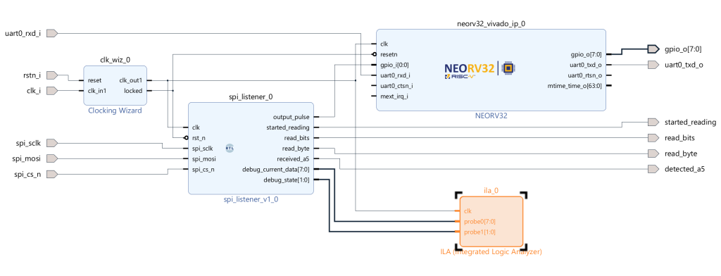
set_property IOSTANDARD LVCMOS33 [get_ports read_byte]Then, we have to add the VHDL functionality to the block design. We could generate a custom IP block for this, but that is a bit of an overkill for a single file design like this. Adding a VHDL file in the form of an RTL (register transfer level) block is simpler. Right-click on the block design canvas, and select “Add Module”. For module type choose “RTL”, and you should have the spi_listener source file listed there. Add it to the design.
While we’re at it, let’s add an integrated logic analyzer block. It should be configured as a native monitor with two probes, one with a width of 8 bits and another with a width of 2 bits. The debug signals will be connected to these. ILA block allows debugging signals during runtime from Vivado, which is handy. I’m not going to show how to use this (because I can’t use it myself that well), but it is a useful block to have on the SoC.
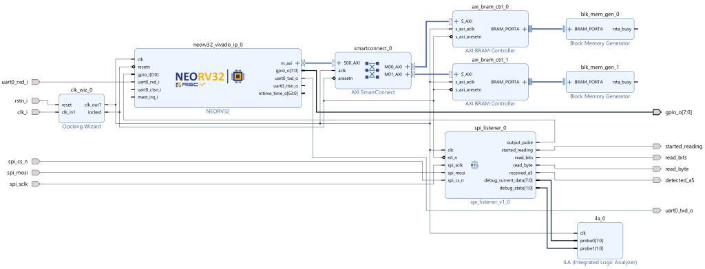
After adding these blocks, wire them up in the following fashion:
You can now generate the bitstream, and program the device. Before getting to the interrupts, let’s first verify that the SPI receiver works.
Testing the SPI Receiver
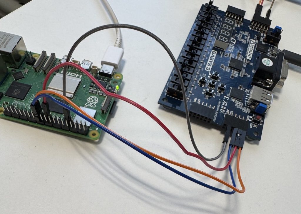
The first thing to do is hook up the SPI receiver to something that can act as an SPI transmitter. I’m using a Raspberry Pi for this purpose. In Raspberry Pi, we first have to enable the SPI by adding dtparam=spi=on to the boot/config.txt. Then we can hook up the two boards together like this:
Once that is done, a simple Python program like this can be used to send the command byte over SPI:
import spidev

spi = spidev.SpiDev()
spi.open(0, 0)  # (bus, device)
spi.max_speed_hz = 1000000  # 1MHz
spi.mode = 0  # SPI mode 0

response = spi.xfer2([0xA5])
print(f"Sent 0xA5, received: {response}")

spi.close()
After running the program above, four LEDs should light up on the FPGA board. The first one indicates transmission has been started, the second one that at least one byte has been read, the third one that a full byte has been received, and finally fourth one that the byte received was the command byte. These LEDs will stay on until the device is reset.
If you’re using Vivado, you should be able to use the logic analyzer as well. For example, it could be interesting to set up a trigger on the debug state changes to see how it changes when a signal is received. This happens in the Trigger Setup tab, but as mentioned, I didn’t dive too deep into this ILA business. With more complex circuits I’d recommend getting familiar with it because it seems quite useful.
One “cool” thing about this is how the SPI receiver and NEORV32 processor are separated. So if you manage to hcf the processor, the SPI receiver will still work and light up the LEDs like nothing has happened (because from its perspective nothing has happened).

Enabling NEORV32 GPIO Interrupts
Some good news and bad news. The good news is that the NEORV32 support is actively being developed in Zephyr, and very recently the GPIO interrupt functionality has been added there. The bad news is that I spent a few days trying to figure out how the NEORV32 interrupts work, wrote a small Zephyr proof-of-concept code to enable the interrupts, and then I wrote this whole chapter about interrupts before realizing the GPIO interrupts now work in the main-branch. I’m not going to remove this chapter, but understanding any of it is not required anymore. That is a good thing, to be honest. But yeah, let the info dump commence.
From the Fast Interrupt Request (FIRQ) chapter in the datasheet, we can see that FIRQ 8 is the number of the GPIO input interrupt. From the datasheet Machine Trap Setup CSRs chapter, we can also see that the FIRQs are enabled by writing to mie (machine interrupt enable) register (shown in “Table 75. mie CSR bits”). FIRQs are the bits 16..31, lower interrupt being a lower bit in the register. Therefore we have to set bit 24 to enable FIRQ 8 to enable the GPIO input interrupts. In case you’re wondering what CSR stands for, it means “Control and Status Register”.
Then, we have to ensure that the machine interrupts are actually enabled. No use in enabling individual interrupts if the interrupts in general are disabled. From “Table 73. mstatus CSR bits” we can see that bit 3 enables the machine-mode interrupts.
Once the GPIO interrupts are enabled, the next step is to configure the individual GPIO interrupt we want to trigger. Do we want it to be edge- or level-triggered, positive or negative? For this, we want to refer to Table 11, “GPIO Trigger Configuration for Pin i”, and Table 12, “GPIO unit register map”. The first table describes the different types of triggers that can be set up. The second table describes the addresses we need to poke to configure the GPIO trigger to the desired behavior. The most interesting are the registers IRQ_TYPE: 0xfffc0010, IRQ_POLARITY: 0xfffc0014 and IRQ_ENABLE: 0xfffc0018. From each register, the nth bit maps to the nth GPIO, so the lowest bit is GPIO 0, etc.
In addition to these, we need to define an interrupt handler, but that is a software detail. We should still take note of the IRQ_PENDING: 0xfffc001c register because the interrupt handler should deal with it.
Now, the moment of truth. Was I smart enough to figure this out by myself? The answer is no. NEORV32 repository has a great GPIO input demo that performs these CPU register setups. All I had to do was cross-reference the example code and datasheet and try to sound smart.
(More good news: the NEORV32 is also actively being developed, so don’t be surprised if the table numbers in the documentation change. The table names seem to be more constant.)
Interrupt Example in Zephyr
Now that we have the hardware capable of receiving an SPI message and generating a GPIO input signal, and an RTOS that is capable of generating GPIO interrupts, let’s combine this all in a Zephyr program, shall we?
As mentioned, the GPIO interrupt support is now in the NEORV32 GPIO driver, and the device tree has the GPIO inputs defined, so all that we need to do is build the GPIO button example. It’s that simple. We don’t have an actual physical button, but the SPI receiver block generates a signal to the NEORV32 GPIO input that is on a logical level the same thing as pressing a button. To compile the button example, we’ll run the following:
west build -p always -b neorv32/neorv32/minimalboot samples/basic/buttonThis is the better option than my proof-of-concept in the sense that my PoC was quite a direct copy of the NEORV32 example code and it did plenty of register poking directly, skipping the whole OS between the application and CPU and going bare-metal. You know you’re doing embedded development when the “hacky solution” is inline assembly in the main. But yes, it’s good to see how this is supposed to be done.
Back to the task at hand. You can now boot Zephyr as instructed in the previous FPGA blog text using serial upload. After Zephyr boots, you should be able to send the command byte from Raspberry Pi to Basys board via SPI, an interrupt should fire, and the message about the event should appear in the serial terminal:
*** Booting Zephyr OS build v4.1.0-3787-ga6ab43aa888b ***
Set up button at gpio@fffc0000 pin 0
Set up LED at gpio@fffc0000 pin 0
Press the button
Button pressed at 291613745
Adding External Memory to NEORV32
One more exercise for our little SoC before giving it some rest. Let’s disable the NEORV32 internal memory, and use external memory instead. Well, external in the sense that it is outside the processor, but internal in the sense that it is still part of our FPGA hardware design. Before that, let’s study a bit more.
AXI
AXI, or Advanced eXtensible Interface, is an on-chip communication bus protocol part of Advanced Microcontroller Bus Architecture (AMBA). The specification is currently in its fourth generation, released in 2010. While the specification is developed by Arm, it is royalty-free and freely available. The fourth version of AXI defines three protocols: AXI4, AXI4-Lite, and AXI4-Stream.
AXI4 and AXI4-Lite are suitable for memory-mapped operations, while AXI4-Stream is quite different from the two and meant for point-to-point data streaming. AXI4 is the most suitable for high-throughput memory interfaces and DMA operations, AXI4-Lite fits better for control registers and configuration spaces, while AXI4-Stream shines for example at video and packet processing.
There are alternatives, of course. For example, Wishbone is an open-source communication bus, and Avalon is Intel’s take on the topic. However, if you’re developing with Vivado, it becomes quite apparent that AXI is the default option. Many IP blocks have AXI interfaces, and the development flow in general leans towards the assumption that you’re using AXI. NEORV32 is Wishbone compatible, but the packaged Vivado block is generated with an AXI bridge to make it more compatible with the Vivado workflow. Since AXI is free, I didn’t go out of my way to try and integrate the more open-source option Wishbone into the block design.
But yes, after all this text, the key takeaway from this is that the AXI is a communication bus.
NEORV32 Memory
From the datasheet, we need to find some information about the memory. Mostly we are interested in the base addresses for the two memory regions that are in the NEORV32 core: instruction memory IMEM and data memory DMEM. These can be found in the chapter 2.6 “Address Space” of the datasheet. From there, we can see that the IMEM starts at 0x0000_0000 and DMEM at 0x8000_0000. Also, this sentence is extremely important:
All accesses to "unmapped" addresses (a.k.a. "the void") are redirected to the Processor-External Bus Interface (XBUS)Once we disable the IMEM and DMEM from the NEORV32 core, the accesses to them become void and are redirected to the external bus. Without this functionality we would not be able to create the external memory blocks, at least not the way it’s shown here.
While you have the datasheet open, I recommend checking out the following tables. Not mandatory, but strongly recommended if you intend to follow along:
- 2.8.1. Instruction Memory (IMEM)
- 2.8.2. Data Memory (DMEM)
- 2.8.7. Processor-External Bus Interface (XBUS)
Updating the Block Design
Since we are working with a block design, the process is quite simple. We need to configure the NEORV32, add AXI bus, add memory blocks, and configure the memory map. After that, we also want to initialize the ROM with our binary, do the wiring, and then we should be good to go. Let’s begin.
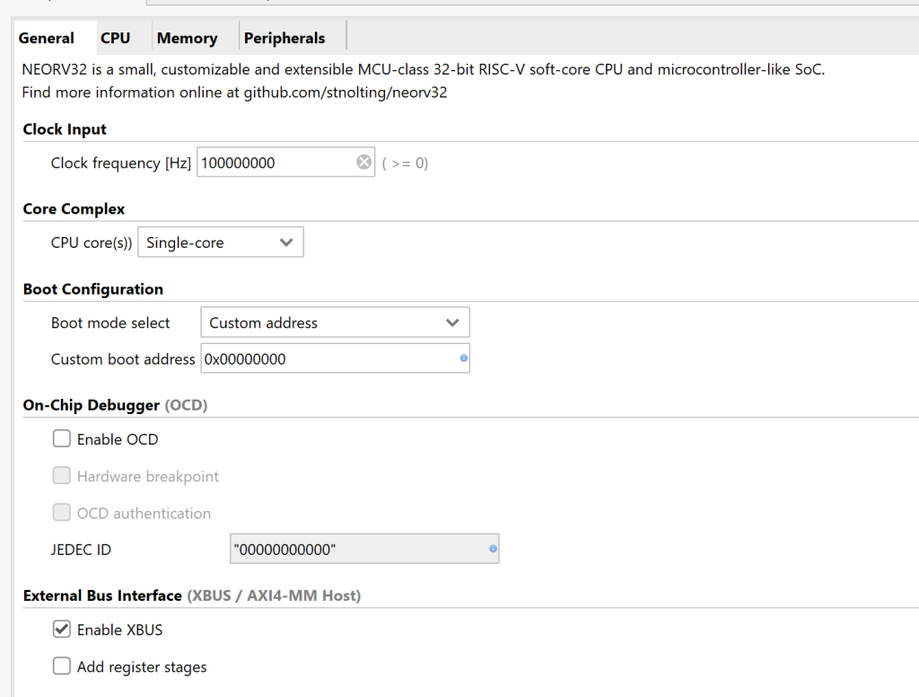
First, double-click on the NEORV32 block, and do the following:
- In Boot Configuration, select Custom Address as boot mode, and
0x00000000as the boot address - Enable the external bus interface by selecting “Enable XBUS”
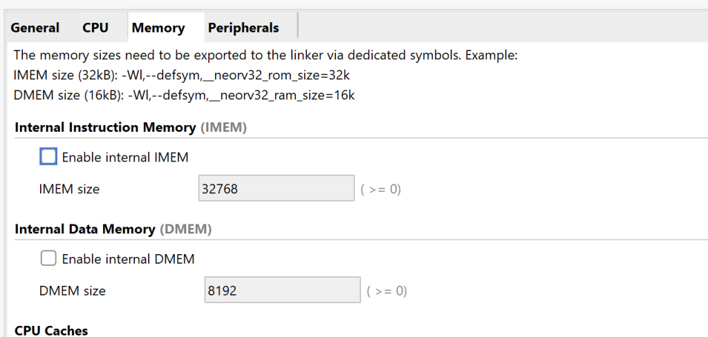
- Disable IMEM and DMEM memories
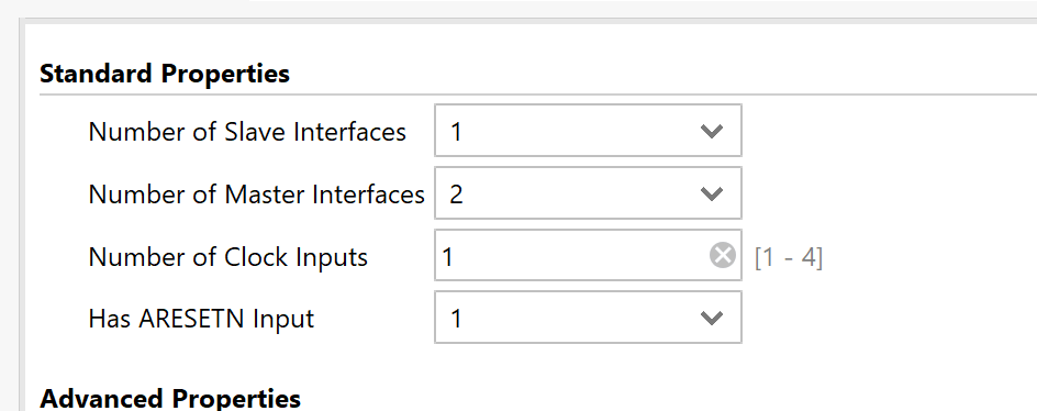
Next, add an AXI SmartConnect block. This block can be used to connect one or more master devices to one or more slave devices. AXI communication happens between one master and one slave device, but the interconnect can be used to expand the number of initiators and targets in the bus. In our case, we have the NEORV32 as the initiator, and two memory blocks as the target (one for IMEM, another for DMEM), and therefore we need an interconnect. Add this, and configure it with one slave interface and two master interfaces.
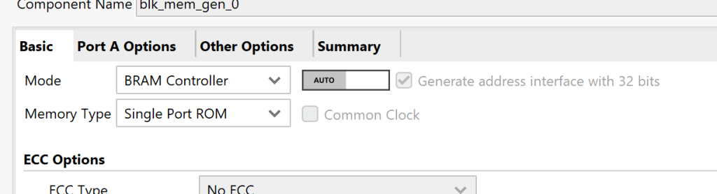
Then, we’ll need two BRAM controllers. Add two AXI BRAM Controller blocks, and configure the Number of BRAM Interfaces to 1. Then add two block memory generators. Configure one of them to be the type of Single Port ROM (this will be IMEM), the other can be left with the default Single Port RAM (this will be DMEM).
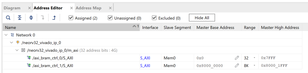
Next, we will need to set up the addresses for the block memories. Open the Address Editor tab from above the block design diagram. Open the hierarchy, select both BRAM controllers, right-click on them, and select “Assign”. The view should reload. Now you should be able to set the Master Base Address and Range for the memory controllers. I chose controller 0 to be the ROM, so I’ll set the Master Base Address 0x0000_0000 and Range 64K. Controller 1 will then be 0x8000_0000 and 8K.
Initiatializing ROM
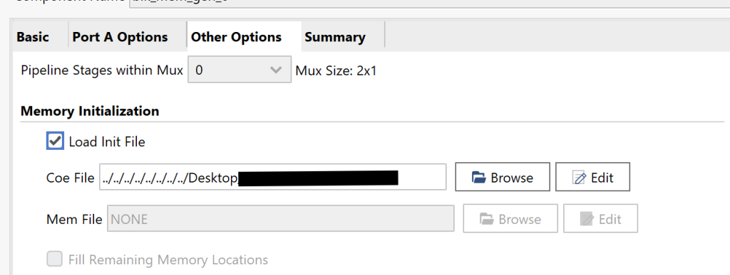
Next, we want to initialize the ROM. So double-click the block memory generator you’ve chosen to be ROM, select Other Options, and check Load Init File.
Now there’s one small problem here with the init file. We cannot use zephyr_exe.bin to initialize memory, as it has the header for the bootloader (and the format in general is wrong). We need to have a Coe file to initialize the ROM. The syntax is fortunately quite simple. Also, we can use the zephyr.vhd generated during the Zephyr build to get the values used to initialize the memory. A little Python script like this can convert the zephyr.vhd file into output.coe file that can be used to initialize the block memory ROM:
#!/usr/bin/python
import re

def convert_vhdl_to_coe(vhdl_path, coe_path):
    with open(vhdl_path, 'r') as file:
        content = file.read()

    # Extract the hex values from the application_init_image_c constant
    match = re.search(r'application_init_image_c\s*:\s*\w+\s*:=\s*\((.*?)\);', content, re.DOTALL)
    if not match:
        raise ValueError("Could not find the application_init_image_c definition.")

    hex_values = re.findall(r'x"([0-9a-fA-F]+)"', match.group(1))

    with open(coe_path, 'w') as file:
        file.write("memory_initialization_radix = 16;\n")
        file.write("memory_initialization_vector =\n")
        for i, value in enumerate(hex_values):
            ending = ',' if i < len(hex_values) - 1 else ';'
            file.write(f"{value.lower()}{ending}\n")

convert_vhdl_to_coe("zephyr.vhd", "output.coe")As a disclaimer, the .coe suffix stands for “coefficients”, and I’m not 100% sure this is the correct way to initialize an SoC ROM. I feel a bit guilty converting an operating system binary into a coefficient file, but it works, so let’s go with it.
Let’s continue on the Vivado side. We were left with the ROM block memory generator open, and the Load Init File option was just enabled. You should now select the output.coe file as the initialization source.
Wiring and Running
Then comes the fun part of wiring all the blocks together. Most of them are quite obvious, like clocks and reset, but getting the AXI part right may be confusing at first. One thing to note is that even though you’re drawing a single line between the AXI initiator and target, multiple ports are being connected. You can use the plus icon next to the port to expand it and see all the signals that are grouped inside it. The result should look like this:
After that, you can perform the usual synthesis, implementation, bitstream generation, and device programming. If everything went according to the plan, you should see the familiar Zephyr boot message in the terminal without the bootloader and manual binary uploading. The instructions get loaded from the block memory defined outside the NEORV32. Great!
One thing worth mentioning: the block design mostly originates from the NEORV32 User Guide, chapter “Packaging the Processor as Vivado IP Block”, where there is a similar Vivado block design screenshot. The NEORV32 guide does not explain how to make the design workable, but it is the basis for the work done here.
Conclusion
Okay, I think I’m done with the FPGA for the time being. It’s a fascinating topic. I feel like I got quite deep into it and still barely scratched the surface. Well, perhaps if I had written the processor myself then I could say I’ve gotten quite deep into it. I hope you found this exploration into the FPGA and Zephyr as fascinating as I did. The next time we will have something more familiar again. Maybe.
Recommended Reading
- All About Circuits: Back to Basics: SPI (Serial Peripheral Interface): Good explanation of SPI with an animation describing how the signals work.
- Five EmbedDev: RISC-V Interrupt Quick Reference: Handy reference of the interrupts in RISC-V. Plenty of other good references as well, if you’re working with RISC-V I guess this would be useful.
- Zephyr: Interrupts: Thorough explanation of the interrupts in Zephyr.
- Nandland: What is Metastability in an FPGA: Brief and understandable explanation of what metastability is and how to fix it. The other FPGA chapters are useful as well, like “What is a Block RAM (BRAM) in an FPGA.“
- Gisselquist Technology: Learning AXI: Where To Start: We didn’t cover AXI much more than just by mentioning that it is a bus, but in case you want to learn more, this is a solid resource.
- AMD: Axi Basics 1 – Introduction to AXI: Quick explanation of what AXI is. The other blog posts in the series are quite useful as well.